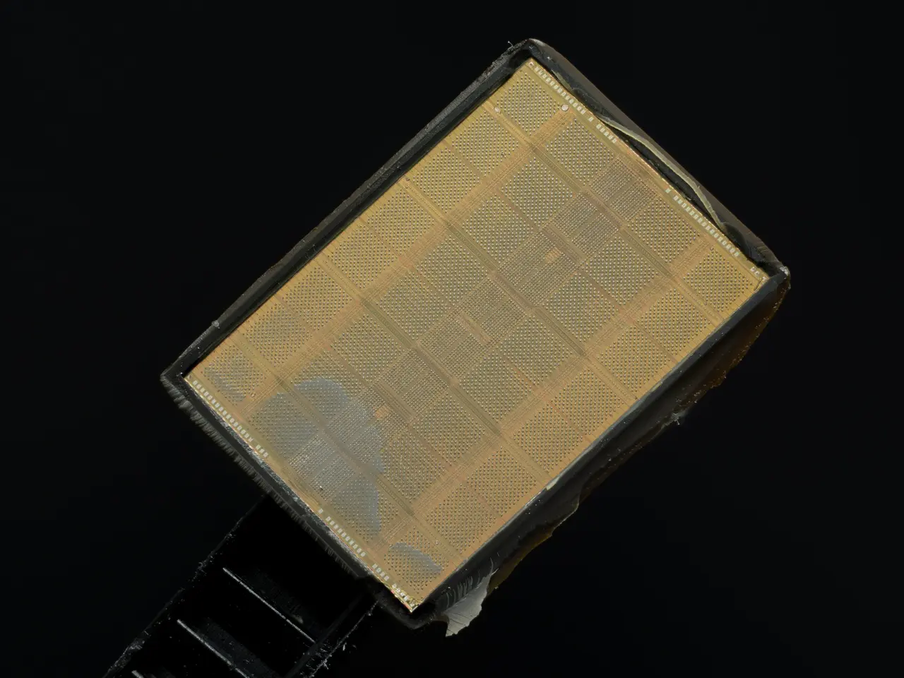
UCLA breakthrough shrinks perovskite energy barrier by 90% for faster electronics
Researchers at UCLA have made a significant breakthrough in improving perovskite semiconductors. The team, led by Xiangfeng Duan, solved a long-standing issue with inefficient electrical current transfer at the metal-perovskite interface. This development could unlock better performance in solar cells, photodetectors, and other electronic devices.
The problem stemmed from a thick energy barrier—around 250 nanometers—between the metal contact and the perovskite layer. Instead of modifying the entire material, the team focused on engineering the microscopic region beneath the metal contact. By creating a van der Waals-laminated metal electrode and exposing it to ultraviolet light, they triggered a controlled diffusion of silver atoms, which then formed silver oxide nanoclusters.
This process formed a localised p-doped domain, shrinking the barrier region to less than 25 nanometers. At this scale, quantum tunnelling (known as Fowler-Nordheim tunnelling) takes over, reducing electrical resistance. The result is faster, more efficient charge transport across the interface.
The method relies on contact-induced doping, where the semiconductor effectively self-modifies through intrinsic chemical and quantum mechanical effects. Unlike traditional approaches, it avoids altering the bulk material, making the solution both elegant and scalable.
The advance remains at the laboratory proof-of-concept stage but provides a clear path forward for perovskite integration. Solar cells could see the most immediate benefits, with improved efficiency and stability expected within the next three to five years. Photodetectors may gain higher sensitivity and quicker response times, while transistors could achieve better mobility and fewer defects. Beyond perovskites, the principles demonstrated could also help address interface challenges in other emerging semiconductor materials.


